Profiles/RecentChanges > PmWiki/PmWiki > Main/HomePage > RelatedTechnology/VerticallyOrientedNanoelectronics
Related Technology: Vertically Oriented Nanoelectronics
Read original article online.
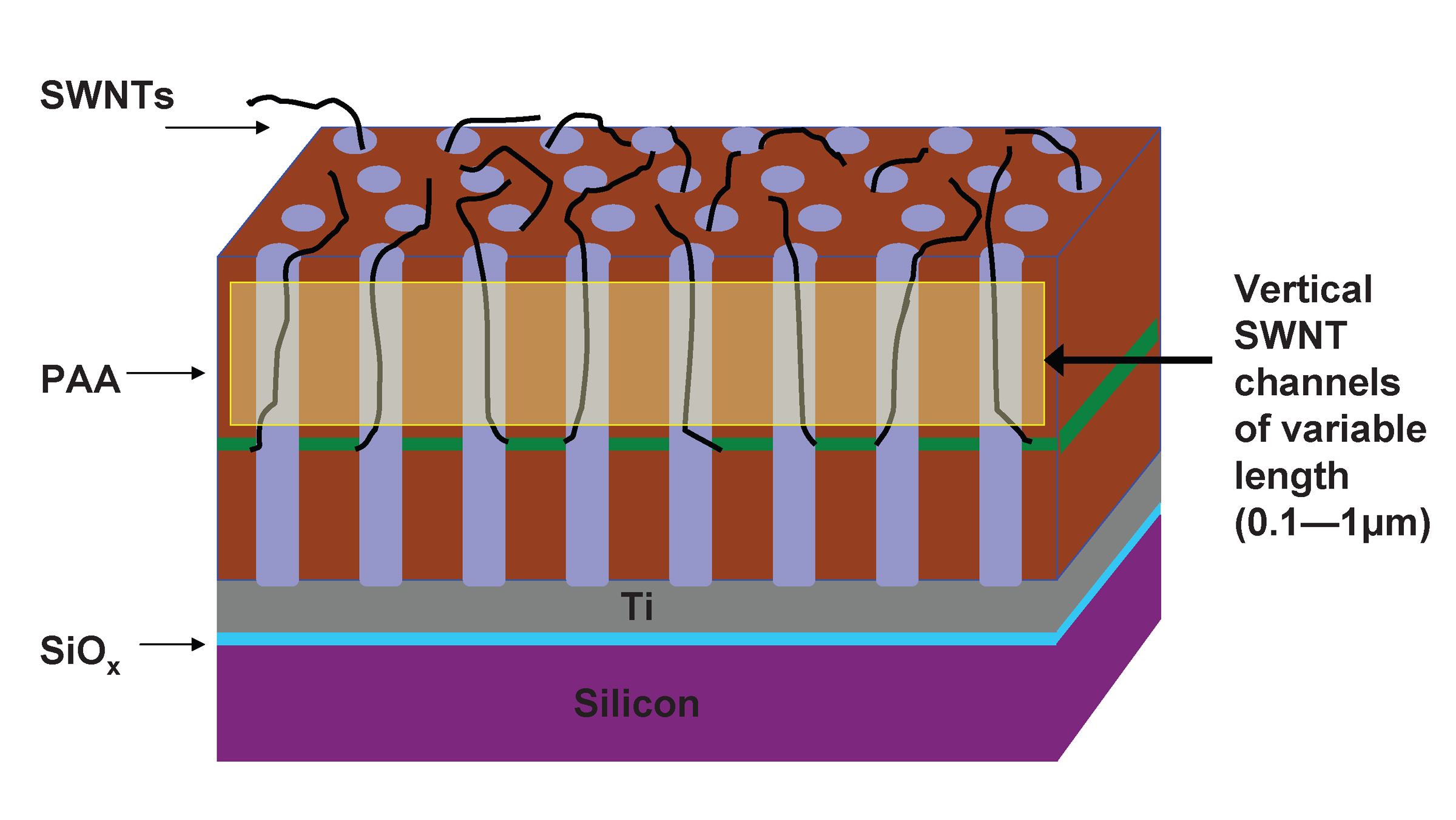
This diagram shows the "porous anodic alumina template" created by Purdue engineers to grow carbon nanotubes vertically out of tiny cavities on top of a silicon wafer. The technique might form a foundation for creating future "vertically oriented" nanoelectronic devices that can pack more devices and circuits into a computer chip while keeping the same footprint size as conventional chips. (Birck Nanotechnology Center, Purdue University)
< Black Silicon | Articles | Self-Powered Silicon Laser Chips >